/ THE SHORT ANSWER
The lab adds domestic post-silicon testing and failure-analysis capacity, including 25,000 sq ft of cleanrooms. Customers should verify certification status, device coverage, queue times, data controls and qualification evidence for the exact service they plan to buy.
- 01HCLTech says it invested Rs 185 crore in a 40,000 sq ft Bengaluru semiconductor lab.
- 02The facility includes 25,000 sq ft of Class 10K and Class 1K cleanrooms.
- 03Its stated scope covers post-silicon engineering, advanced testing and failure analysis.
- 04Target certifications and vendor-listed equipment do not yet prove throughput or acceptance performance.
/ dotSuper point of view
A functioning lab is stronger evidence than a policy ambition, but semiconductor programmes should be evaluated by accepted qualification work, not floor area or equipment lists.
What changed
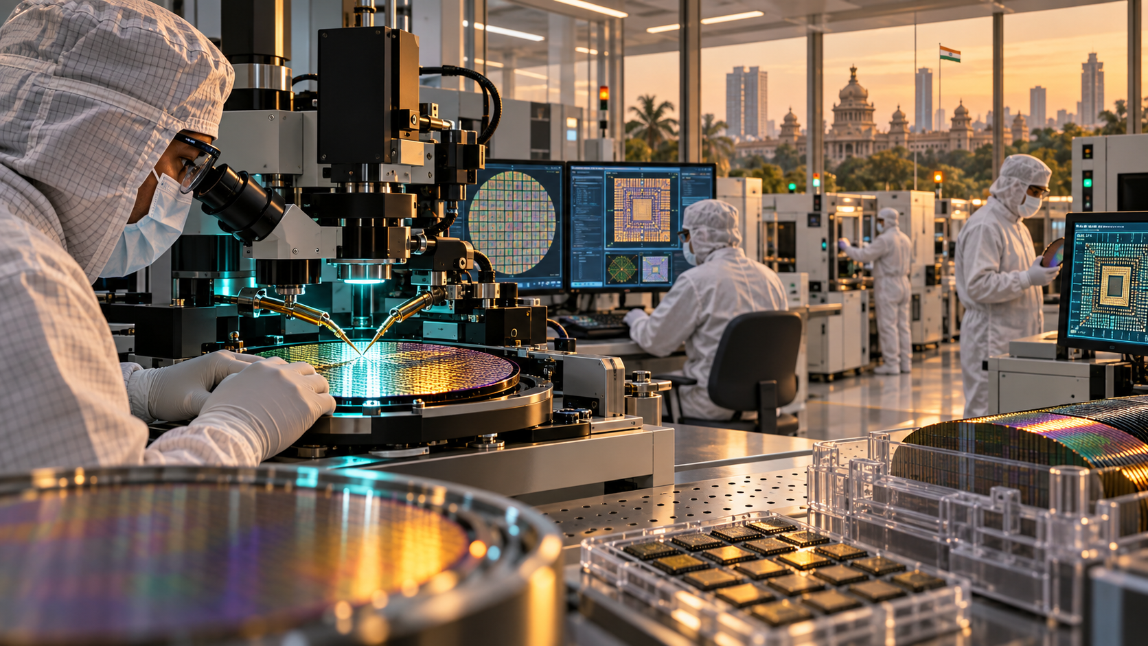
HCLTech announced on 8 September that it has opened an Advanced Semiconductor Lab in Bengaluru with an investment of Rs 185 crore. The company describes the 40,000 sq ft facility as an integrated site for post-silicon engineering, advanced testing and failure analysis.
HCLTech says 25,000 sq ft is dedicated to Class 10K and Class 1K cleanrooms. The listed equipment includes automated test systems, probes, qualification chambers, optical and electron microscopy, and focused ion beam systems from established testing and instrumentation suppliers.
The company positions the lab within its Spec2Parts model, covering work from electrical validation and automated testing through qualification and failure analysis. It also says the site will serve Indian and international customers across research, pre-production and production qualification.
- Confirmed: the Bengaluru facility has been launched and its investment, floor area and intended capabilities are disclosed.
- Planned: HCLTech says it expects certifications including ISO 17025, ISO 9001, AS 9100 and ISO 13485.
- Not disclosed: current utilisation, customer queue, test throughput, accepted-device range and completed qualification results.
The qualification test for customers
The facility can reduce the need to coordinate separate providers for validation, testing and failure analysis. For Indian chip, electronics, automotive, aerospace and medical-device teams, domestic access could shorten logistics and improve collaboration during design-debug cycles.
Those benefits depend on the exact device and process. A cleanroom classification or equipment brand does not show whether the lab supports a customer's package type, voltage range, test temperature, reliability standard or production volume. Certification targets also need to be separated from certifications already granted.
Sensitive semiconductor work creates an information-security requirement alongside technical capability. Customers should understand how designs, test programmes, wafer maps, failure images and production data are segregated, retained and accessed across the service workflow.
- Compare accepted turnaround time and first-pass completion, not only installed equipment.
- Confirm which certifications are active for the purchased scope.
- Review data segregation, export-control and intellectual-property handling.
- Ask for representative qualification evidence under comparable device conditions.
What semiconductor teams should do next
Prepare a service matrix before engaging the lab. Define the device, package, wafer size, interfaces, environmental conditions, reliability standard, expected volumes, failure-analysis depth and evidence required for customer or regulator acceptance.
Request a scoped capability review tied to that matrix. The review should identify available equipment, calibration status, operator competence, applicable certifications, queue time, data boundary, subcontracted steps and the format of final reports.
Begin with a bounded qualification or failure-analysis job and set acceptance criteria in advance. Measure turnaround, repeatability, defect resolution, evidence quality and handoff effort before moving a larger programme.
- Use one representative device as the first proof point.
- Record every external handoff that remains outside the integrated workflow.
- Require a named owner for technical exceptions and data handling.
- Expand only after the first job meets documented acceptance criteria.
What this page cannot conclude
- 01The available sources do not disclose current customer utilisation or completed production qualification programmes.
- 02The certifications named by HCLTech are expected targets and should not be treated as already granted without verification.
- 03Equipment availability does not establish compatibility with every device, package or reliability standard.
- 04Commercial pricing, queue times and service-level commitments require direct supplier due diligence.
Sources
- 01HCLTech launches Advanced Semiconductor Lab with Rs. 185 crore investmentHCLTech · accessed Sep 9, 2026
- 02HCLTech invests Rs 185 crore to launch advanced semiconductor lab in BengaluruMoneycontrol · accessed Sep 9, 2026
- 03HCLTech launches Advanced Semiconductor Lab in BengaluruThe Week · accessed Sep 9, 2026
Our editorial standard · Found an error? Send a correction with its source.
/ CITE OR SHARE THIS GUIDE
Make the evidence easy to verify.
When you reference this guide, link to its canonical URL. That gives readers one stable place for the evidence, limitations and future updates.
dotSuper Research Desk. (September 9, 2026). HCLTech opened a Rs 185 crore semiconductor lab. Buyers should test qualification capacity.. dotSuper. https://dotsuper.net/feeds/daily-briefing/2026-09-09-hcltech-semiconductor-lab